Charleston Gardens in Palo Alto in Santa Clara County, California — The American West (Pacific Coastal)
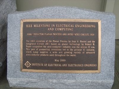
Semiconductor Planar Process and Integrated Circuit
IEEE Milestone in Electrical Engineering and Computing
— 1959 —
Inscription.
The 1959 invention of the Planar Process by Jean A. Hoerni and the Integrated Circuit (IC) based on planar technology by Robert N. Noyce catapulted the semiconductor industry into the silicon IC era. This pair of pioneering inventions lead to the present IC industry which today supplies a wide and growing variety of advanced semiconductor products used throughout the world.
Erected 2009 by Institute of Electrical and Electronics Engineers.
Topics and series. This historical marker is listed in these topic lists: Industry & Commerce • Science & Medicine. In addition, it is included in the IEEE Milestones in Electrical Engineering and Computing series list. A significant historical year for this entry is 1959.
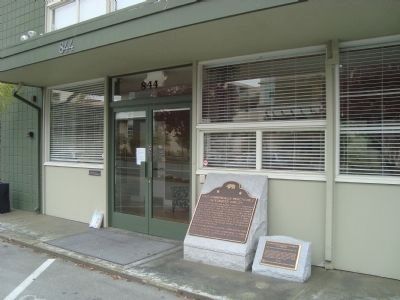
Location. 37° 25.309′ N, 122° 6.2′ W. Marker is in Palo Alto, California, in Santa Clara County. It is in Charleston Gardens. Marker is on East Charlston Road west of San Antonio Road, on the left when traveling west. Touch for map. Marker is at or near this postal address: 844 East Charlston Road, Palo Alto CA 94303, United States of America. Touch for directions.
Other nearby markers. At least 8 other markers are within 2 miles of this marker, measured as the crow flies. First Commercially Practicable Integrated Circuit (here, next to this marker); El Palo Nuevo (approx. 0.6 miles away); J. Pearce Mitchell Park (approx. ¾ mile away); Star Steel Windmill (approx. 0.8 miles away); Immigrant House (approx. 0.8 miles away); Rengstorff House (approx. 1.1 miles away); The Spirit of the Times (approx. 1.1 miles away); Birthplace of Silicon Valley (approx. 1.3 miles away). Touch for a list and map of all markers in Palo Alto.
Credits. This page was last revised on February 7, 2023. It was originally submitted on March 31, 2012, by Barry Swackhamer of Brentwood, California. This page has been viewed 771 times since then and 22 times this year. Photos: 1, 2. submitted on March 31, 2012, by Barry Swackhamer of Brentwood, California. • Syd Whittle was the editor who published this page.

