Mountain View in Santa Clara County, California — The American West (Pacific Coastal)
Birthplace of Silicon Valley
IEEE Milestone
— 1956 —
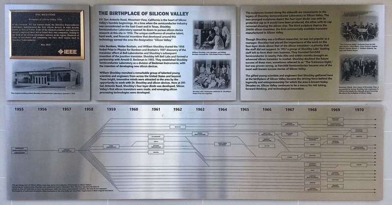
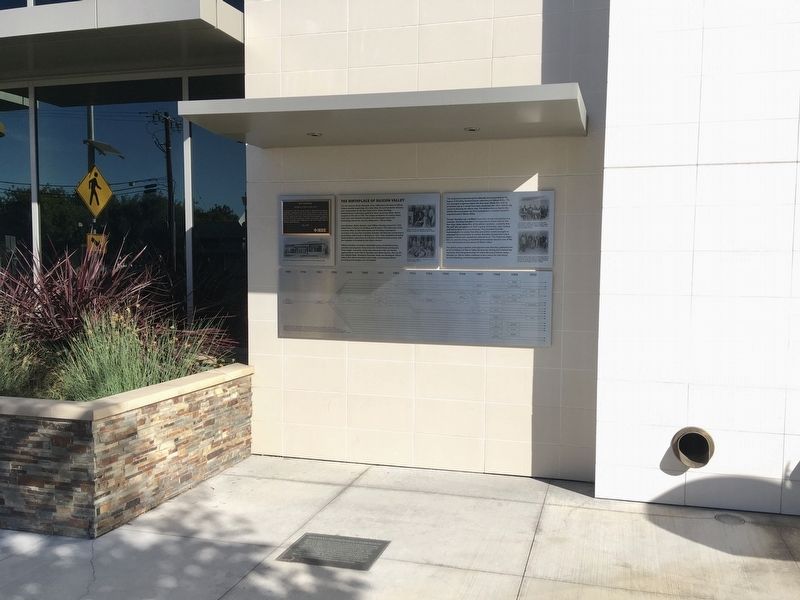
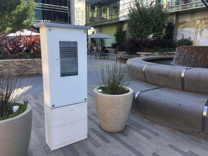
At this location, 391 San Antonio Road, the Shockley Semiconductor Laboratory manufactured the first silicon devices in what became known as Silicon Valley. Some of the talented scientists and engineers initially employed there left to found their own companies, leading to the birth of the silicon electronics industry in the region. Hundreds of firms in electronics and computing can trace their origins back to Shockley Semiconductor.
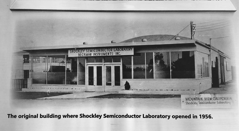
391 San Antonio Road, Mountain View, California, is the heart of Silicon Valley's humble beginnings. At a time when the semiconductor industry was concentrated on the East Coast and in Texas, Shockley Semiconductor Laboratory opened its doors to pursue silicon device research at this site in 1956. The unique confluence of creative talent, hard work, and financial incentives that developed around this technology earned the area the designation "Silicon Valley."
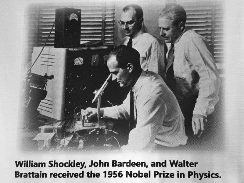
John Bardeen, Walter Brattain, and William Shockley shared the 1956 Nobel Prize in Physics for Bardeen and Brattain's 1947 discovery of the transistor effect at Bell Laboratories and Shockley's subsequent invention of the junction transistor. Shockley left Bell Labs and formed a partnership with Arnold O. Beckman in 1955. They established Shockley Semiconductor Laboratory as a division of Beckman Instruments, with the intention of developing new silicon devices.
William Shockley recruited a remarkable group of talented young scientists and engineers from across the United States and beyond. These bright, innovative minds were attracted to the area by the opportunity to work with Dr. Shockley and silicon devices. Here at 391 San Antonio Road, Shockley's four-layer diode was developed, Silicon Valley's first silicon transistors were made, and emerging silicon processing technologies were developed.
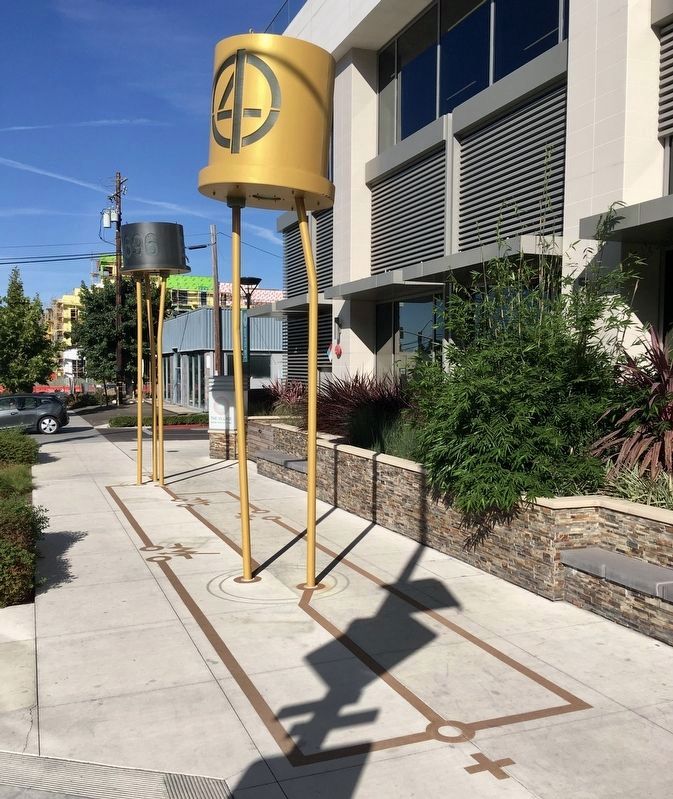
The sculptures located along the sidewalk are monuments to the legacy of Shockley Semiconductor Laboratory in Silicon Valley. The two-pronged sculptures depict the four-layer diode: one with its protective cap as it would have been produced, the other with its cap removed showing the silicon chip. The third sculpture depicts the 2N696 silicon transistor, the first commercially available transistor manufactured in Silicon Valley.
Though Shockley was a brilliant researcher, he was not popular as a manager. Shockley had placed the importance of the work on the four-layer diode above that of the silicon transistor — a priority that the staff did not support. In 1957 a group of Shockley Labs' leading staff left to form their own business. They founded Fairchild Semiconductor in nearby Palo Alto and within months brought an advanced silicon transistor to market. Shockley doubted the future success of these men, sometimes referred to as "The Traitorous Eight," but was proven wrong, as Fairchild Semiconductor became one of the most well-known success stories of Silicon Valley.
The gifted young scientists and engineers that Shockley gathered here at the birthplace of Silicon Valley became the driving force behind the ingenuity and entrepreneurship for which the area is known today. Decades on, Silicon Valley continues to be a mecca for risk taking, forward thinking, and technological innovation.
caption:
This genealogy chart of Silicon Valley's early days shows the explosion of businesses in Silicon Valley's semiconductor industry after Shockley Labs established itself in Mountain View. The lines represent the flow of people as they left their jobs to form new businesses within the area's semiconductor industry; the lines do not represent the longevity of individual companies. Many businesses in the area today can trace their origins back to these original innovators.
Erected 2018 by Institute of Electrical and Electronics Engineers.
Topics and series. This historical marker is listed in these topic lists: Industry & Commerce • Science & Medicine. In addition, it is included in the IEEE Milestones in Electrical Engineering and Computing series list.
Location. 37° 24.291′ N, 122° 6.676′ W. Marker is in Mountain View, California, in Santa Clara County. Marker is on San Antonio Road, 0.3 miles north of El Camino Real, on the right when traveling north. Touch for map. Marker is at or near this postal address: 391 San Antonio Rd, Mountain View CA 94040, United States of America. Touch for directions.
Other nearby markers. At least 8 other markers are within 2 miles of this marker, measured as the crow flies. Mariano Castro Adobe (approx. ¾ mile away); Mayfield Fire Bell (approx. 0.8 miles away); Juana Briones. This is her park. (approx. 0.9 miles away); Juana Briones Park (approx. 0.9 miles away); El Palo Nuevo (approx. 1.1 miles away); Immigrant House (approx. 1.2 miles away); Star Steel Windmill (approx. 1.2 miles away); First Commercially Practicable Integrated Circuit (approx. 1.3 miles away). Touch for a list and map of all markers in Mountain View.
Credits. This page was last revised on November 10, 2021. It was originally submitted on September 27, 2021, by Craig Baker of Sylmar, California. This page has been viewed 1,007 times since then and 117 times this year. Photos: 1, 2, 3, 4, 5, 6. submitted on September 27, 2021, by Craig Baker of Sylmar, California.
